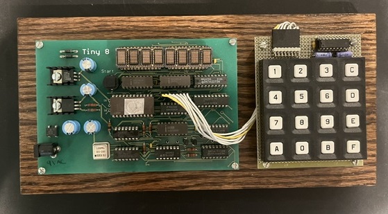
The Tiny 8 is Jim Kearney's single-board Intel 8008 computer (copyright 2002, tiny8@jkearney.com). Design goal: the simplest possible 8008 that still has RAM, EPROM, a display, and a port. Kearney's phrase was "minimal but powerful," with some slightly anachronistic LSTTL and CMOS around a PMOS CPU. The MicroBasement unit has a keyboard on the input port. Firmware is his Tiny 8 Demo and Monitor Program.
Kearney also reconstructed a Mark-8 (new PCBs, period parts, his own switch board) and wrote an 8008 assembler for Windows. The Tiny 8 is the compact machine from that same bench. Manual, schematic, and layout were part of the project package.
The 8008 is pMOS: +5 V and -9 V. An external AC transformer feeds two half-wave supplies. An LM7805 makes +5 (two diodes drop heat on the regulator). An LM337 makes -9. Filter caps are oversized because of the half-wave feed.
A 1 MHz oscillator module is divided by half of a 74LS74 and two NOR gates (1/2 74LS02) into phi-1 and phi-2, 180 degrees apart, 500 ns wide. The data sheet wants about 700 ns and 550 ns. Kearney ran 500 ns and it held over normal temperatures. Pull-ups bring LSTTL highs up to the 3.5 V the 8008 wants.
A 74LS138 (IC11) decodes CPU state during SYNC and phi-2. The design uses T1, T2, and T3 only: ST1 and ST2 latch the multiplexed address bytes in two 74LS273s (IC4, IC6); ST3 is the data window. Pressing reset asserts INT. The second half of the 74LS74 synchronizes it per the data sheet. The 273s clear to zero, so the next fetch is from location 0 and must be a one-byte RST to load the program counter.
IC14 decodes A12/A13 and one cycle-control bit during T3. Four 4 KB read strobes and four write strobes. No INP/OUT instructions; ports live in the map. Devices smaller than 4 KB appear more than once (the 1 KB RAM is mapped four times in its block).
A daughterboard can stack on a wire-wrap EPROM socket. Pads exist for the extra address bit and the 2nd/3rd-block strobes. The on-board supply will not feed the second card.
Two ways in: burn an EPROM, or type into RAM from the optional keyboard (this unit has the keyboard). Addresses below are octal, as in Kearney's assembler.
Reset clears the address latches, so fetch 0 must be a one-byte RST that jumps to the real start:
	code
	org	0
	rst	1	; INT / reset lands here
	org	10B	; transfers here
	... your program ...
RAM base is 30000B. Leave the last 16 bytes alone (warm-reset vector lives there). Max user code 1008 bytes. The monitor starts a RAM program; you do not need the RST-at-zero header.
	code
	org	30000B
	... your program ...
Write ASCII to 24B through 33B, right to left on the pair of displays. Example: H=0, L=33B, then LMI "H", DCL, LMI "e", and so on for "Hello". Control registers are 04B and 10B (see the display data sheet). Those addresses sit in the same 4 KB as the EPROM, so if H already points at ROM you can skip LHI.
Read 20000B. Six bits of port data: upper three and lower three. Middle two bits are unused. Keyboard on this machine feeds that port.
After firmware has run once, reset goes through a RAM vector at 031762B. Monitor mode points it back at the monitor. A RAM program can retarget it.
On power-up the stock EPROM:
During that scroll:
Source and Intel hex for that EPROM exist with the project files.
Mark-8 and SCELBI-8B are 1974 8008 machines. The Tiny 8 is a 2002 one-board 8008 with a monitor you can type at. Same multiplexed bus, same RST-at-zero reset trick, far fewer chips than a Mark-8.